Home > Semiconductors & Electronics > IC > Thin Wafer Market
Thin Wafer Market Analysis
- Report ID: GMI5007
- Published Date: Mar 2021
- Report Format: PDF
Thin Wafer Market Analysis
The 100μm - 199μm wafer dominated more than 50% of the market share in 2020 and will showcase growth rate of 6% till 2027 owing to its rising acceptance in memory devices as majority of the memory architecture thickness varies from 100 - 300 μm. Although the thickness of memory devices varies among the packaging technology and application requirements.
DRAM and 2D NAND flash memory manufacturers use thin silicon wafers with a thickness of 150 μm or above. The development of 3D stacked memory is further influencing the market players to adapt <150 μm substrates as they deliver compact and cost-effective packaging options. This will further enhance the market opportunities for 100μm-199μm thin wafers.
The 200 mm thin wafer held 40% of the market share in 2020 and will grow at a CAGR of around 7.50% through 2027. 200 mm wafers are experiencing a rising adoption among the market leaders of power devices such as Metal-Oxide-Semiconductor Field-Effect Transistor (MOSFET), Insulated-Gate Bipolar Transistor (IGBT), and Radio Frequency (RF) devices. Increasing demand for power semiconductors in IoT, 5G, and autonomous transportation will foster the market value for thin wafer manufacturers.
To cater to the high demand in the industry, wafer manufacturers are planning several strategic initiatives. For example, in September 2019, Cree, Inc. expanded its wafer fabrication facility with the introduction of a 200mm production plant in North Carolina. This new facility will produce 200 mm wafers for RF devices and power semiconductors. Continuous technological innovation in the thin wafer industry will further propel the growth opportunities for wafer manufacturers.

The temporary bonding and debonding in the thin wafer market accounted for USD 250 million in 2020 and is predicted to attain a CAGR of 7% by 2027. Market participants are widely adopting the bonding and debonding technology as it delivers high throughput, low cost, and low wafer stress during processing.
The temporary bonding & debonding process delivers improved mechanical support in handling the solution for ultra-thin wafers. This process improves the miniaturization property and increases thin wafer demand in compact semiconductor devices for IoT, data centers, and autonomous vehicles. To cater to the high demand in the market, companies are focusing on technology enhancement, creating a growth opportunity for wafer manufacturers.

The LED segment will hold 20% of the thin wafer market share by 2027. LED manufacturers majorly adopt thin wafers in the backend process to remove extra substrates and improve the miniaturization property. The market is majorly driven by the emerging applications in the LED segment such as Vertical-Cavity Surface-Emitting Laser (VCSEL).
Majority of the VCSEL manufacturers are adopting 150 mm wafer size to deliver improved militarization property with better heat management. Increasing demand for VCSEL in emerging applications, such as augmented reality and face recognition in smartphones, will accelerate the market potential in the coming years. The demand will encourage VCSEL manufacturers to adopt various business expansion strategies to gain a high competitive edge.

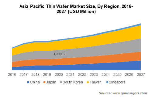
South Korea thin wafer market accounted for over 25% of revenue share in 2020 and is poised to expand at a CAGR of more than 6% between 2021 and 2027 driven by the presence of major semiconductor manufacturers in the region such as Samsung, SK Hynix, and ON Semiconductor, among others. Additionally, rising government initiatives along with funding activities have further accelerated the growth opportunity for thin wafer manufacturing.

