Summary
Table of Content

Thin Wafer Processing & Dicing Equipment Market
Get a free sample of this report
Form submitted successfully!
Error submitting form. Please try again.
Thank you!
Your inquiry has been received. Our team will reach out to you with the required details via email. To ensure that you don't miss their response, kindly remember to check your spam folder as well!

Request Sectional Data
Thank you!
Your inquiry has been received. Our team will reach out to you with the required details via email. To ensure that you don't miss their response, kindly remember to check your spam folder as well!
Form submitted successfully!
Error submitting form. Please try again.
Thin Wafer Processing & Dicing Equipment Market Size
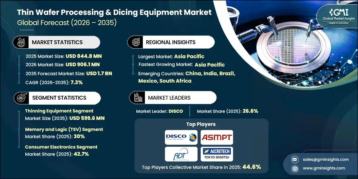
The global thin wafer processing & dicing equipment market was estimated at USD 844.8 million in 2025. The market is expected to grow from USD 906.1 million in 2026 to USD 1.3 billion in 2031 and USD 1.7 billion by 2035, at a CAGR of 7.3% during the forecast period of 2026–2035, according to the latest report published by Global Market Insights Inc.

To get key market trends
The accelerating adoption of electric vehicles is creating demand for advanced semiconductor devices. The International Energy Association predicts that over 20 million electric units will be sold in 2025, making 25% of the global vehicle market. The first quarter of 2025 showed more than a 35% year-on-year growth. Such increasing number of vehicles being produced and assembled is driving the demand of processors, sensors, and advanced control systems, and subsequently the need for ultra-thin wafers, improved yield, and high-reliability backend processing solutions.
The advent of 5G, electric vehicles, and new materials, such as silicon carbide (SiC) and gallium nitride (GaN), significantly increase the need for high-precision wafer processing that facilitates microchip and sensor manufacturing. The development of laser-based dicing technologies, which are faster, more precise, and cost- effective is growing, in order to meet the demand for thinner and durable semiconductor components. Aligning to this trend, Lidrotec received USD 1 million in follow-on funding and was awarded Company of the Year for the Luminate 2022 Finals in March 2023. The company is able to successfully address the demand in the market for equipment used in the processing and cutting of thin wafers with their patented laser technology used for wafer cutting.
Wafer processing and dicing equipment consists of machines that thin silicon wafers and then precisely cut them into single chips. These tools facilitate the development of compact, high-performing semiconductors for 5G, electronics, automotive, and computing.
Thin Wafer Processing & Dicing Equipment Market Report Attributes
| Key Takeaway | Details |
|---|---|
| Market Size & Growth | |
| Base Year | 2025 |
| Market Size in 2025 | USD 844.8 Million |
| Market Size in 2026 | USD 906.1 Million |
| Forecast Period 2026-2035 CAGR | 7.3% |
| Market Size in 2035 | USD 1.7 Billion |
| Key Market Trends | |
| Drivers | Impact |
| Rising demand for miniaturized electronic devices | Drives the need for ultra-thin wafers and high-precision dicing, increasing demand for advanced wafer processing equipment. |
| Proliferation of 5G and high-performance computing applications | Expands semiconductor production requirements, boosting adoption of precision wafer thinning and high-throughput dicing solutions. |
| Increased use of advanced semiconductor materials | Necessitates specialized handling and cutting technologies, enhancing market demand for equipment capable of processing new materials. |
| Growth in automotive electronics and EVs | Elevates demand for power devices, sensors, and control ICs, driving wafer processing and dicing equipment adoption. |
| Pitfalls & Challenges | Impact |
| High costs of advanced dicing equipment | Limits adoption among smaller manufacturers, potentially slowing market growth in cost-sensitive regions. |
| Increased fragility of thinned wafers | Increases the need for precise handling and stress-minimizing equipment, creating opportunities for specialized solutions. |
| Opportunities: | Impact |
| Integration of artificial intelligence and automation in wafer handling | Improves yield, efficiency, and process reliability, accelerating equipment adoption in high-volume manufacturing. |
| Improves yield, efficiency, and process reliability, accelerating equipment adoption in high-volume manufacturing. | Improves yield, efficiency, and process reliability, accelerating equipment adoption in high-volume manufacturing. |
| Market Leaders (2025) | |
| Market Leaders |
26.6% market share in 2025 |
| Top Players |
|
| Competitive Edge |
|
| Regional Insights | |
| Largest Market | Asia Pacific |
| Fastest growing market | Asia Pacific |
| Emerging countries | China, India, Brazil, Mexico, South Africa |
| Future outlook |
|
What are the growth opportunities in this market?
Thin Wafer Processing & Dicing Equipment Market Trends
- One of the most important trends affecting the thin wafer processing and dicing equipment market is the increased use of modern packaging technologies. These technologies, including 2.5D and 3D ICs and heterogeneous integration, require precise wafer thinning and high-precision dicing.
- Equipment manufacturers are focusing on the development of laser dicing and plasma dicing, which offer higher yields and allow processing of extremely thin and delicate wafers, in order to reduce mechanical stress during the wafer dicing process.
- The need for improved edge quality, higher throughput, and more dimensional control in equipment manufacturing is being driven by miniaturization and increased chip density.
- Automation and artificial intelligence are improving operational efficiencies, and decreasing downtimes in process control, defect detection, and predictive maintenance in the backend semiconductor manufacturing.
- The focus on yield improvement and on reducing costs is resulting in the implementation of advanced wafer handling systems and utilization of temporary bonding and debonding techniques, especially in high-volume manufacturing settings.
Thin Wafer Processing & Dicing Equipment Market Analysis

Learn more about the key segments shaping this market
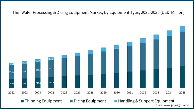
On the basis of equipment type, the thin wafer processing and dicing equipment market is divided into thinning equipment, dicing equipment, and handling and support equipment.
- The thinning equipment segment is anticipated to reach USD 599.6 million by 2035. As semiconductor manufacturers strive for more compact ultra-thin wafers and high-performance devices, the demand for thinning equipment is increasing. The recent improvements made in the areas of precision grinding, as well as in chemical mechanical polishing (CMP) are resulting in higher yields, reduced wafer stress, and improved compatibility with fragile wafers. These developments are especially beneficial for high-density memory, power devices, and advanced packaging applications.
- The dicing equipment segment was valued at USD 459.6 million in 2025 and is anticipated to grow at a CAGR of 7.2% over the forecast years. A recent trend in wafer dicing equipment focuses on laser and plasma dicing technologies due to their ability to improve edge quality and chip loss on ultra-thin wafers. Automated and AI-optimized control systems are being used to boost throughput and yield of complex semiconductor devices such as MEMS, TSVs, and power ICs.

Learn more about the key segments shaping this market
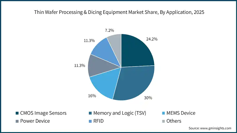
On the basis of application, the thin wafer processing & dicing equipment market is segmented into CMOS image sensors, memory and logic (TSV), MEMS devices, power devices, RFIDs, and others.
- The memory and logic (TSV) segment held a market share of 30% in 2025. High-precision thinning and dicing equipment is increasingly in demand for TSV (Through-silicon via) memory and logic devices. Trends include improved wafer handling and control of mechanical stress and laser cutting of fine pitch TSVs. Automated processes and management have become essential to meet the complex requirements of the design of 3D integrated circuits and systems in packages.
- The MEMS devices segment is anticipated to grow at a CAGR of 8.6% during the forecast period 2026 - 2035. The MEMS devices segment continues to grow exponentially, and this is largely due to the increasing interest and application in the automotive sensors, industrial automation systems, and in consumer electronics. Some of the more recent trends include the use of ultra-thin wafer processing, high precision plasma and laser dicing, and advanced systems to reduce mechanical stress. Automation and real-time tracking mechanisms are being used to improve yield and reliability.
On the basis of end use industry, the thin wafer processing & dicing equipment market is divided into consumer electronics, automotive, telecommunications, healthcare, aerospace and defense, industrial, and others.
- The consumer electronics segment held a market share of 42.7% in 2025. The expansion of consumer electronic devices increases the need for semiconductors that are thinner, lighter, and provide better performance. The precise wafer slicing and high-speed cutting required for the manufacture of smartphones, tablets, and wearable devices push the industry's use of more sophisticated automation and laser technology, better quality control through AI, and rapid deployment of all processing systems.
- The automotive segment is anticipated to grow at a CAGR of 8.2% during the forecast period 2026 - 2035. The automotive segment, particularly electric and autonomous vehicles, is increasing wafer-level demand for power devices, sensors, and control ICs. Trends include robust handling solutions for large, thin wafers, high-precision dicing, and integration of automated inspection to ensure reliability and yield for safety-critical applications under high-volume production environments.

Looking for region specific data?
The North America thin wafer processing & dicing equipment market held a 26.3% share of the global market in 2025.
- The North American thin wafer processing and dicing equipment market is currently experiencing the increasing adoption of cutting-edge semiconductor manufacturing technologies due to the high demand from consumer electronics, automotive, and high-performance computing industries.
- To support the growing domestic demand for automated semiconductor fabrication, investments in automation, laser dicing, and ultra-thin wafer processing are accelerating.
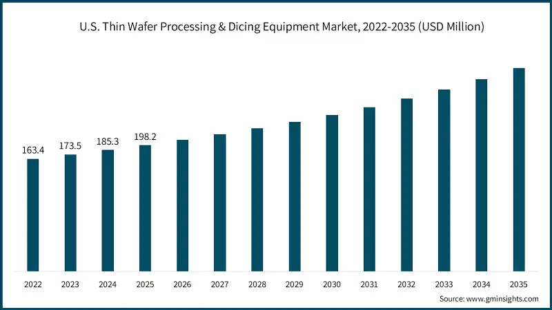
The U.S. thin wafer processing & dicing equipment market was valued at USD 163.4 million and USD 173.5 million in 2022 and 2023, respectively. The market size reached USD 198.2 million in 2025, growing from USD 185.3 million in 2024.
- The U.S. market is driven by increasing semiconductor content in electric vehicles and consumer electronics. According to Statista, the electric vehicles market in the United States is projected to reach a revenue of USD 105.8 billion in 2025.
- This is boosting demand for thinning, dicing, and handling equipment to support power devices, sensors, and control ICs.
Europe thin wafer processing & dicing equipment market accounted for USD 161.4 million in 2025 and is anticipated to show lucrative growth over the forecast period.
- Europe’s thin wafer processing and dicing equipment market is growing steadily, supported by increasing demand for advanced packaging and high-performance semiconductor devices. The automotive industry, consumer electronics, and industrial automation are the primary industries fueling the growth of the sector.
- To improve efficiency and yield, manufacturers deploy laser and plasma dicing technologies, ultra-thin wafer handling systems, and AI-based process monitoring. Market stimulation is derived from government support for the advanced electronics and semiconductor fabrication and research. In addition, the shift to miniaturized, high-density devices drives the investment in precision wafer processing and back-end systems.
Germany dominates the Europe thin wafer processing & dicing equipment market, showcasing strong growth potential.
- The markets for thin wafer processing and dicing equipment are positively impacted by the automotive and consumer electronics markets in Germany. According to GTAI, Germany’s consumer electronics was anticipated to reach approximately 30.34 billion USD in 2024, which demonstrates growing opportunities in the market.
- Increasing demand for electric cars, efficient computing, and industrial automation is accelerating the uptake of wafer thinning, laser-based dicing, and automation handling technologies.
- Manufacturers are focusing their efforts on investing in optimal and advanced wafer processing equipment as well as semiconductor backend systems in order to meet industry demands.
The Asia Pacific thin wafer processing & dicing equipment market is anticipated to grow at the highest CAGR of 8.3% during the analysis timeframe.
- Asia Pacific dominates the thin wafer processing and dicing equipment market, driven by semiconductor manufacturing hubs in China, Taiwan, Japan, and South Korea. The implementation of high-precision wafer thinning, laser dicing, and automated handling systems is driven by strong demand in smartphones, memory chips, automotive electronics, and 5G devices.
- Manufacturers are investing in AI-enabled process control and predictive maintenance to improve yield and throughput.
China thin wafer processing & dicing equipment market is estimated to grow with a significant CAGR, in the Asia Pacific market.
- China’s thin wafer processing and dicing equipment market is growing rapidly due to increasing domestic semiconductor fabrication and advanced packaging initiatives.
- Consumer electronics, automotive electronics, and 5G applications drive demand, while government policies encouraging chip self-sufficiency and large-scale manufacturing expansion increase the demand for precision thinning and dicing. Manufacturers are concentrating on laser and non-contact dicing, ultra-thin wafer handling, and automation to increase yields and lower defects. This trend supports the region's high-volume production and advanced device manufacturing.
Brazil leads the Latin American thin wafer processing & dicing equipment market, exhibiting remarkable growth during the analysis period.
- The Brazilian market for the processing and dicing of thin wafers is expanding rapidly, driven by the subsequent expansion of automotive electronics, consumer electronics and industrial automation industries.
- Rising domestic assembly and the initiatives to import semiconductors have led to the demand for laser dicing, wafer thinning, and automated handling to provide precise solutions. There is an increasing trend among manufacturers to invest in systems that provide high yield and reliability for thin and fragile components. Combined with investment in backend semiconductor manufacturing and domestic industrial development initiatives, Brazil is strengthening its position in high-precision wafer processing.
South Africa thin wafer processing & dicing equipment market to experience substantial growth in the Middle East and Africa market in 2025.
- Industrial automation, automotive electronics, and consumer electronics are driving the thin wafer processing and dicing equipment market in South Africa. Technologies like ultra-thin wafer processing, laser dicing, and automated handling are gradually being adopted to fulfill local manufacturing needs.
- To address local manufacturing needs, technologies like laser dicing and automated handling are slowly being adopted. Precision, equipment reliability, and yield optimization are the key focus of manufacturers to address the needs of small and medium scale semiconductor production. Regional expansion in automotive as well as high-value electronics applications is further stimulating demand for the more advanced wafer processing and dicing equipment.
Thin Wafer Processing & Dicing Equipment Market Share
Key competitors in the thin wafer processing and dicing equipment market consider multiple factors, including product innovation, precision, reliability, and advanced automation capabilities. To satisfy the demands of semiconductor fabrication and packaging, manufacturers concentrate on differentiated equipment offerings, such as laser-based dicing, handling of ultra-thin wafers, and high-throughput solutions. Market players such as DISCO, ASMPT, Advanced Dicing, and TOKYO SEIMITSU collectively accounted for a significant share of 44.6% in the global thin wafer processing and dicing equipment market in 2025, reflecting intense competition. Alongside maintaining high precision and yield, companies emphasize reducing operational costs, enhancing process efficiency, and integrating AI-enabled monitoring. These companies capitalize on the strong market demand for new technologies in the packaging of semiconductor devices to gain a competitive advantage.
Thin Wafer Processing & Dicing Equipment Market Companies
Prominent players operating in the thin wafer processing & dicing equipment industry are as mentioned below:
- Advanced Dicing Technologies
- ASMPT
- AXUS TECHNOLOGY
- Citizen Chiba Precision Co., Ltd.
- DISCO Corporation
- Dynatex International
- EV Group (EVG)
- HANMI Semiconductor
- Han's Laser Technology Co., Ltd.
- KLA Corporation
- Lam Research Corporation
- DISCO
DISCO is a leading player in the thin wafer processing and dicing equipment market with a market share of approximately 26.6%. The company specializes in precision engineering, high-throughput wafer thinning, and advanced laser-based dicing solutions to meet the semiconductor manufacturers’ processing needs for ultra-thin wafers, high yield, and effective backend processing.
ASMPT holds a significant market share of around 11.1% in the thin wafer processing and dicing equipment market. The company specializes in automated wafer handling, advanced dicing systems, and integrated process solutions in order to maximize productivity and precision and improve reliability in all areas of semiconductor manufacturing and packaging.
Advanced Dicing commands a market share of approximately 2.0% in the thin wafer processing and dicing equipment market. The company specializes in laser and plasma dicing technologies, offering high-precision solutions for delicate wafers, emphasizing efficiency, minimal wafer stress, and improved yield for semiconductor device manufacturers.
Thin Wafer Processing & Dicing Equipment Industry News
- In October 2024, MKS Instruments unveiled plans to establish its first Asian factory in Penang, Malaysia, dedicated to the production of thin wafer processing and dicing equipment. This facility, designated as a super center, will be constructed in three phases, significantly enhancing the company’s semiconductor manufacturing capabilities while creating high-value jobs in the region.
- In May 2024 Lam Research announced its expansion in the semiconductor fabrication equipment supply chain in India, targeting the thin wafer processing & dicing equipment industry. The company aimed to source precision parts and gas delivery systems, expressing openness to government incentives to enhance its local operations.
The thin wafer processing & dicing equipment market research report includes in-depth coverage of the industry with estimates and forecast in terms of revenue in USD Million from 2022 – 2035 for the following segments:
Market, By Equipment Type
- Thinning equipment
- Dicing equipment
- Blade dicing
- Laser dicing
- Stealth dicing
- Plasma dicing
- Handling & support equipment
- Temporary bonding/debonding systems
- Wafer mounting/demounting systems
- Cleaning & inspection systems
Market, By Wafer Size
- Less than 4 inch
- 5 inch and 6 inch
- 8 inch
- 12 inch
Market, By Wafer Thickness
- 750 µm (standard / less thin)
- 120 µm (advanced mainstream)
- 50 µm and below
Market, By Application
- CMOS image sensors
- Memory and logic (TSV)
- MEMS device
- Power device
- RFID
- Others
Market, By End Use Industry
- Consumer electronics
- Automotive
- Telecommunications
- Healthcare
- Aerospace & defense
- Industrial
- Others
The above information is provided for the following regions and countries:
- North America
- U.S.
- Canada
- Europe
- Germany
- UK
- France
- Spain
- Italy
- Netherlands
- Asia Pacific
- China
- India
- Japan
- Australia
- South Korea
- Latin America
- Brazil
- Mexico
- Argentina
- Middle East and Africa
- South Africa
- Saudi Arabia
- UAE
Frequently Asked Question(FAQ) :
What is the growth outlook for the MEMS devices application segment?
What is the growth outlook for the MEMS devices application segment?
What is the U.S. thin wafer processing & dicing equipment market size in 2025?
The U.S. market was valued at USD 198.2 million in 2025, supported by strong semiconductor manufacturing activity and rising adoption of advanced wafer thinning and precision dicing technologies.
What are the upcoming trends in the thin wafer processing & dicing equipment industry?
Key trends include adoption of laser and plasma dicing technologies, integration of AI and automation in wafer handling, growth of advanced packaging (2.5D/3D ICs), and increasing focus on ultra-thin wafer processing to improve yield and reliability.
How much revenue did the dicing equipment segment generate in 2025?
The dicing equipment segment was valued at USD 459.6 million in 2025, supported by increasing adoption of laser and plasma dicing technologies for ultra-thin and fragile semiconductor wafers.
What is the outlook for the thinning equipment segment by 2035?
The thinning equipment segment is anticipated to reach USD 599.6 million by 2035, driven by demand for ultra-thin wafers, improved yield, and compatibility with advanced packaging and high-density semiconductor devices.
Who are the key players in the thin wafer processing & dicing equipment market?
Key players include DISCO Corporation, ASMPT, Advanced Dicing Technologies, TOKYO SEIMITSU, KLA Corporation, Lam Research Corporation, Han’s Laser Technology, EV Group (EVG), and HANMI Semiconductor.
What is the projected value of the thin wafer processing & dicing equipment market by 2035?
The market size for thin wafer processing & dicing equipment is expected to reach USD 1.7 billion by 2035, growing at a CAGR of 7.3%. This expansion is driven by growth in electric vehicles, 5G deployment, advanced packaging technologies, and high-performance computing applications.
What is the market size of the thin wafer processing & dicing equipment industry in 2026?
The market size for thin wafer processing & dicing equipment reached USD 906.1 million in 2026, reflecting increased adoption of precision wafer thinning and high-throughput dicing solutions.
What is the thin wafer processing & dicing equipment market size in 2025?
The market size for thin wafer processing & dicing equipment was valued at USD 844.8 million in 2025. Rising demand for miniaturized electronic devices and advanced semiconductor manufacturing is supporting steady market growth.
Thin Wafer Processing & Dicing Equipment Market Scope
Related Reports


